A Field-programmable Gate Array (FPGA) is an integrated circuit designed to be configured by the customer or designer after manufacturing—hence "field-programmable". The FPGA configuration is generally specified using a hardware description language (HDL), similar to that used for an application-specific integrated circuit (ASIC) (circuit diagrams were previously used to specify the configuration, as they were for ASICs, but this is increasingly rare). FPGAs can be used to implement any logical function that an ASIC could perform. The ability to update the functionality after shipping, partial re-configuration of the portion of the design and the low non-recurring engineering costs relative to an ASIC design (notwithstanding the generally higher unit cost), offer advantages for many applications.
FPGAs contain programmable logic components called "logic blocks", and a hierarchy of reconfigurable interconnects that allow the blocks to be "wired together"—somewhat like many (changeable) logic gates that can be inter-wired in (many) different configurations . Logic blocks can be configured to perform complexcombinational functions, or merely simple logic gates like AND and XOR. In most FPGAs, the logic blocks also include memory elements, which may be simple flip-flops or more complete blocks of memory.
In addition to digital functions, some FPGAs have analog features. The most common analog feature is programmable slew rate and drive strength on each output pin, allowing the engineer to set slow rates on lightly loaded pins that would otherwisering unacceptably, and to set stronger, faster rates on heavily loaded pins on high-speed channels that would otherwise run too slow. Another relatively common analog feature is differential comparators on input pins designed to be connected todifferential signaling channels. A few "mixed signal FPGAs" have integrated peripheral Analog-to-Digital Converters (ADCs) and Digital-to-Analog Converters (DACs) with analog signal conditioning blocks allowing them to operate as a system-on-a-chip. Such devices blur the line between an FPGA, which carries digital ones and zeros on its internal programmable interconnect fabric, and field-programmable analog array (FPAA), which carries analog values on its internal programmable interconnect fabric.
Definitions - A field-programmable gate array (FPGA) is an integrated circuit (IC) that can be programmed in the field after manufacture. FPGAs are similar in principle to, but have vastly wider potential application than, programmable read-only memory (PROM) chips. FPGAs are used by engineers in the design of specialized ICs that can later be produced hard-wired in large quantities for distribution to computer manufacturers and end users. Ultimately, FPGAs might allow computer users to tailor microprocessors to meet their own individual needs.Architecture - The most common FPGA architecture consists of an array of logic blocks (called Configurable Logic Block, CLB, or Logic Array Block, LAB, depending on vendor), I/O pads, and routing channels. Generally, all the routing channels have the same width (number of wires). Multiple I/O pads may fit into the height of one row or the width of one column in the array.
An application circuit must be mapped into an FPGA with adequate resources. While the number of CLBs/LABs and I/Os required is easily determined from the design, the number of routing tracks needed may vary considerably even among designs with the same amount of logic. For example, a crossbar switch requires much more routing than a systolic array with the same gate count. Since unused routing tracks increase the cost (and decrease the performance) of the part without providing any benefit, FPGA manufacturers try to provide just enough tracks so that most designs that will fit in terms of LUTs and IOs can be routed. This is determined by estimates such as those derived fromRent's rule or by experiments with existing designs.
In general, a logic block (CLB or LAB) consists of a few logical cells (called ALM, LE, Slice etc). A typical cell consists of a 4-input Lookup table(LUT), a Full adder (FA) and a D-type flip-flop, as shown below. The LUT are in this figure split into two 3-input LUTs. In normal mode those are combined into a 4-input LUT through the left mux. In arithmetic mode, their outputs are fed to the FA. The selection of mode are programmed into the middle mux. The output can be either synchronous or asynchronous, depending on the programming of the mux to the right, in the figure example. In practice, entire or parts of the FA are put as functions into the LUTs in order to save space.
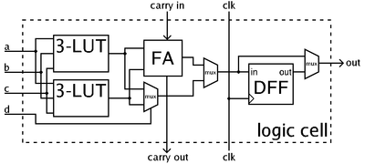
ALMs and Slices usually contains 2 or 4 structures similar to the example figure, with some shared signals.
CLBs/LABs typically contains a few ALMs/LEs/Slices.
In recent years, manufacturers have started moving to 6-input LUTs in their high performance parts, claiming increased performance.
Since clock signals (and often other high-fanout signals) are normally routed via special-purpose dedicated routing networks in commercial FPGAs, they and other signals are separately managed.
For this example architecture, the locations of the FPGA logic block pins are shown below.
Each input is accessible from one side of the logic block, while the output pin can connect to routing wires in both the channel to the right and the channel below the logic block.
Each logic block output pin can connect to any of the wiring segments in the channels adjacent to it.
Similarly, an I/O pad can connect to any one of the wiring segments in the channel adjacent to it. For example, an I/O pad at the top of the chip can connect to any of the W wires (where W is the channel width) in the horizontal channel immediately below it.
Generally, the FPGA routing is unsegmented. That is, each wiring segment spans only one logic block before it terminates in a switch box. By turning on some of the programmable switches within a switch box, longer paths can be constructed. For higher speed interconnect, some FPGA architectures use longer routing lines that span multiple logic blocks.
Whenever a vertical and a horizontal channel intersect, there is a switch box. In this architecture, when a wire enters a switch box, there are three programmable switches that allow it to connect to three other wires in adjacent channel segments. The pattern, or topology, of switches used in this architecture is the planar or domain-based switch box topology. In this switch box topology, a wire in track number one connects only to wires in track number one in adjacent channel segments, wires in track number 2 connect only to other wires in track number 2 and so on. The figure below illustrates the connections in a switch box.

Modern FPGA families expand upon the above capabilities to include higher level functionality fixed into the silicon. Having these common functions embedded into the silicon reduces the area required and gives those functions increased speed compared to building them from primitives. Examples of these include multipliers, generic DSP blocks, embedded processors, high speed IO logic and embedded memories.
FPGAs are also widely used for systems validation including pre-silicon validation, post-silicon validation, and firmware development. This allows chip companies to validate their design before the chip is produced in the factory, reducing the time-to-market.
Credit :
ไม่มีความคิดเห็น:
แสดงความคิดเห็น